AI Visual Inspection in Electronics Manufacturing

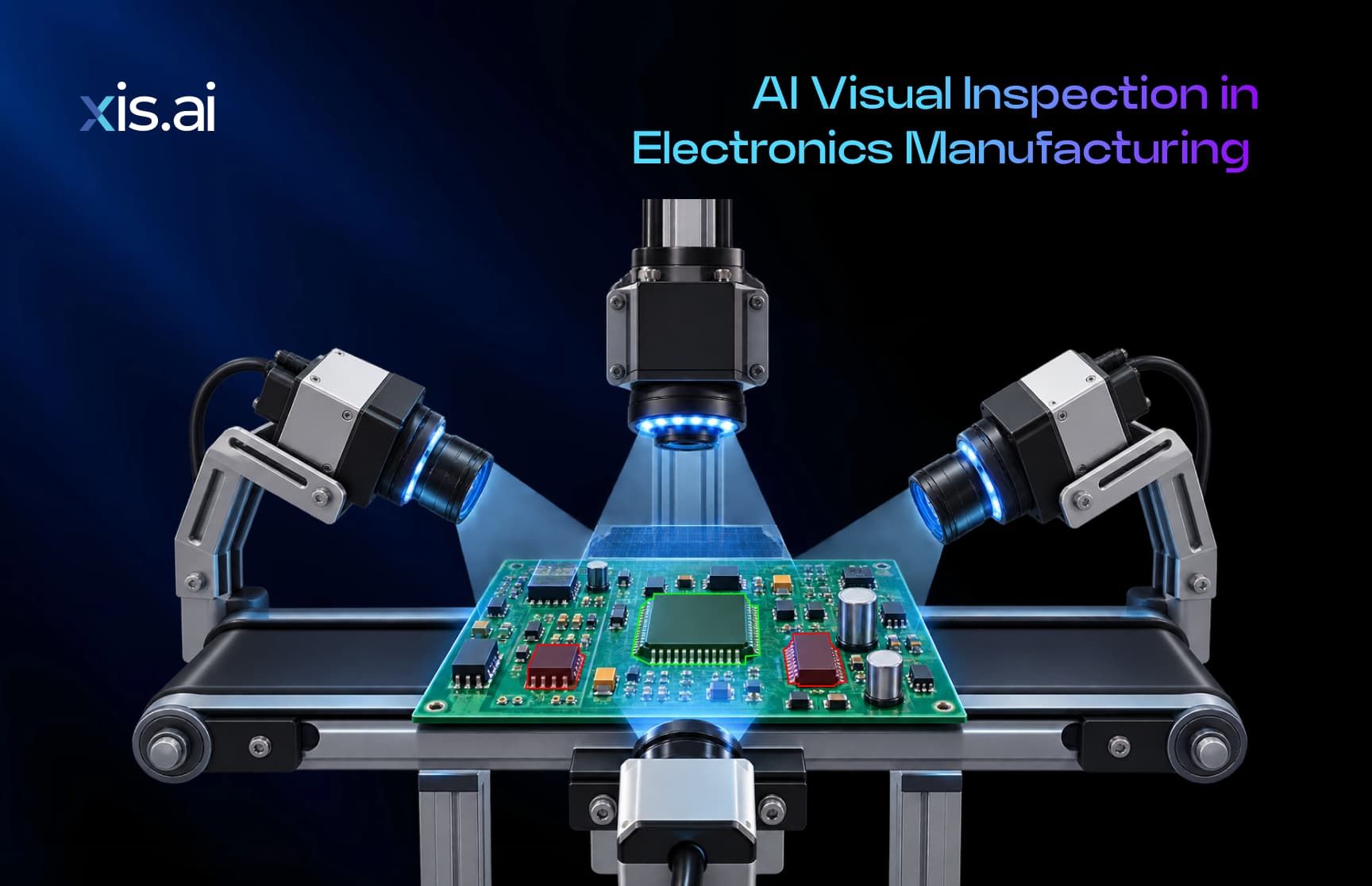
Electronics manufacturing runs on tolerances that human eyes were never built to catch consistently. A single misaligned component, an insufficient solder joint, or a hairline wafer defect can pass an inspector's glance and still cause a product to fail months later in the field. As component density increases and production speeds climb, manual visual checks and rule-based Automated Optical Inspection are reaching their limits. AI visual inspection in electronics manufacturing addresses this gap directly, applying trained, consistent standards to every unit at every stage of the production line rather than relying on periodic sampling or inspector judgment.
This guide walks through how AI-powered inspection applies across the five stages that matter most in electronics production: PCB inspection, SMT inspection, solder joint inspection, semiconductor inspection, and connector inspection. Each stage catches a different category of defect, and together they form a complete quality control chain from bare board to finished assembly.
What AI Visual Inspection Means for Electronics Manufacturing
AI visual inspection uses computer vision and deep learning models to analyze images captured during production and flag defects that fall outside a trained standard. Unlike fixed-rule Automated Optical Inspection, which compares pixel values against tolerances, AI-based systems learn the range of normal variation and identify genuine anomalies within it. This distinction matters most in electronics manufacturing, where defect types are subtle, production runs vary across board designs, and false rejects carry a real cost in scrap and rework.
Platforms such as xis.ai deploy these models directly at the edge, on industrial cameras or local processing units positioned on the line itself, so inspection decisions happen at full production speed without sending data to a centralized server first.
PCB Inspection: Catching Defects Before Assembly Begins
Printed circuit boards form the foundation every other inspection stage builds on. Bare-board defects such as etching irregularities, trace breaks, and surface contamination are far cheaper to catch before components are placed than after. AI-driven PCB inspection analyzes board images at production speed, learning to distinguish acceptable manufacturing variation from genuine defects that manual visual checks and legacy Automated Optical Inspection routinely miss at high line speeds. For a closer look at how this stage works, see PCB Defect Detection Is No Longer Just About Quality Control.
SMT Inspection: Verifying Component Placement at Speed
Once components are placed, Surface-Mount Technology inspection verifies that every part sits correctly before the board moves to reflow. Component misplacement, polarity errors, and missing parts are common at this stage, and they compound quickly if not caught immediately, since a single placement error can affect every downstream process step. AI-based SMT inspection analyzes placement images in real time, flagging deviations that rule-based systems often pass through as acceptable variation. A detailed breakdown of this stage is available in AI SMT Inspection Systems: Why Electronics Manufacturers Are Rethinking Quality Control.
Solder Joint Inspection: Ensuring Reliable Connections
Solder joints determine whether an assembly holds up over its full service life, and they remain one of the hardest defect categories to catch through manual review. A joint that looks acceptable under one lighting angle can hide insufficient solder or a hairline bridge visible only from another angle. AI solder joint inspection applies a consistent trained standard to every joint on every board, catching insufficient solder, bridging, and misalignment regardless of shift or individual inspector judgment. This stage is covered in depth in AI Solder Joint Inspection for Electronics Manufacturing.
Semiconductor Inspection: Detecting Defects at the Chip Level
Semiconductor inspection operates at a finer scale than board-level checks, examining wafers, dies, and packaged devices for particles, pattern breaks, and micro-cracks that threaten yield. Because defect tolerances at the chip level are measured in microns rather than millimeters, this stage depends heavily on high-resolution imaging paired with models trained specifically on chip-level defect patterns rather than general board defects. AI-based semiconductor inspection extends the same consistency principle seen at the PCB and SMT stages down to the component level itself, closing a gap that rule-based tools struggle with as node sizes shrink.
Connector Inspection: Protecting Signal and Power Integrity
Connectors are a common point of field failure precisely because their defects are easy to overlook visually. Bent pins, incomplete seating, contamination, and plating defects rarely show up as an obvious rejection under standard lighting, yet any one of them can cause an intermittent signal or power failure well after a product ships. AI connector inspection applies the same full-coverage, consistent-standard approach used earlier in the line to this final assembly point, reducing the field-failure risk that manual spot-checks tend to miss.
Building a Unified Electronics Inspection Strategy
Treating these five stages as a connected chain, rather than five separate checkpoints, gives manufacturers a fuller picture of where defects originate and why. A recurring solder issue traced back to a stencil problem, or a connector failure traced back to an upstream placement error, becomes visible only when inspection data across stages is viewed together. This is the direction platforms like xis.ai are built for: no-code deployment across every stage of electronics production, with models trained per stage but working from the same underlying inspection philosophy. For a broader view of how AI inspection generates operational insight beyond pass/fail sorting, see Industrial Vision Systems Explained: Components, Benefits, and Applications.
Frequently Asked Questions
What is AI visual inspection in electronics manufacturing?
It is the use of computer vision and deep learning to automatically detect defects in electronic boards, components, and assemblies, replacing or supplementing manual checks and rule-based Automated Optical Inspection.
Which electronics manufacturing stage benefits most from AI inspection?
Every stage benefits, but solder joint and semiconductor inspection see the largest gains, since defects at these stages are the hardest for manual review to catch consistently.
Can AI inspection run at full production line speed?
Yes. Edge AI platforms such as xis.ai run inspection models locally on the production line, allowing real-time defect detection without slowing throughput.
Does AI inspection replace Automated Optical Inspection entirely?
Not necessarily. AI-based inspection often supplements existing Automated Optical Inspection systems, adding the ability to catch subtle or previously unseen defect types that fixed-rule systems miss.
How does AI inspection reduce field failures in electronics products?
By applying a consistent trained standard across every unit at every stage, AI inspection catches defects such as connector seating issues or solder bridging before assembly moves forward, reducing the defects that would otherwise surface only after a product reaches the customer.
Comment
0Comments
No comments yet.