AI Semiconductor Defect Detection

What Is Semiconductor Defect Detection?
Semiconductor defect detection involves identifying flaws on a wafer, die, or finished chip prior to advancement to subsequent fabrication or assembly stages. Defects at this scale may include particle contamination on the wafer surface, misaligned photolithography patterns, cracks propagating through a die, or bonding faults at the package level. Since semiconductor devices are constructed in layers, defects introduced early in the process are compounded by each subsequent step. Therefore, detection speed and coverage are as critical as detection accuracy.
Semiconductor manufacturing occurs at a scale where conventional visual inspection rapidly reaches its physical limitations. Circuit features on modern wafers are measured in nanometers, a resolution beyond standard camera and lens systems without specialized optics. Defect rates that are negligible in other manufacturing sectors can result in substantial yield loss when multiplied across wafers containing thousands of individual die. Consequently, semiconductor quality control has long relied on specialized inspection equipment. The current shift is from fixed-rule image comparison to trained AI models that learn to identify defects, rather than relying solely on predefined checklists.
How Semiconductor Wafer Inspection Works
Semiconductor wafer inspection typically happens at several checkpoints across the fabrication sequence, not as a single final check. Bare wafer inspection screens incoming material for surface contamination or crystal defects before any patterning begins. In-line inspection occurs between individual process steps, such as after etching or deposition, to catch pattern deviations while they can still be corrected or the affected wafer scrapped early rather than late. Final inspection, often paired with electrical test, evaluates completed die before packaging.
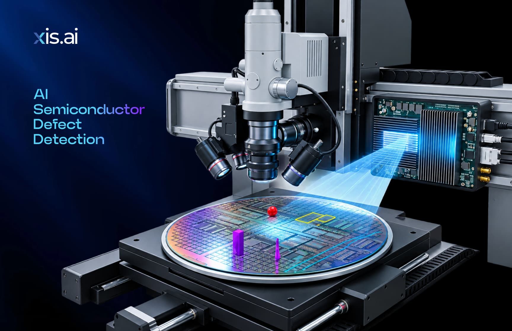
At each of these checkpoints, high-resolution imaging, whether from optical microscopy, scanning electron microscopy, or specialized dark-field and bright-field systems, captures the wafer surface or pattern layer. An AI-based inspection model compares this image data against a learned reference of what a defect-free pattern looks like, flagging deviations for review. This is the same anomaly-based logic xis.ai applies in PCB defect detection, where a model trained on normal appearance flags departures from it rather than checking against a fixed list of known defect types.
Wafer surface defects fall into a few recurring categories that inspection systems are trained to recognize:
- Particle contamination — foreign material deposited during handling or processing, which can bridge circuit features or block subsequent patterning steps
- Pattern defects — misalignment, bridging, or incomplete etching in the photolithography layer
- Crystal-originated defects — flaws present in the silicon substrate itself, often invisible until later processing exposes them
- Scratches and mechanical damage — surface damage from wafer handling, transport, or polishing steps
- Film non-uniformity — inconsistent thickness or composition in deposited layers, which affects device performance even without a visible physical flaw
Why Micro Defect Detection Matters at This Scale
The economics of semiconductor manufacturing are fundamentally driven by yield, defined as the proportion of die on a wafer that pass final testing and are suitable for sale. Since a single wafer represents significant production value, even minor improvements in defect capture rates can substantially reduce the cost per functional die. Consequently, micro defect detection—identifying flaws at the sub-micron scale—is regarded as a core yield-management function rather than merely a downstream quality checkpoint.
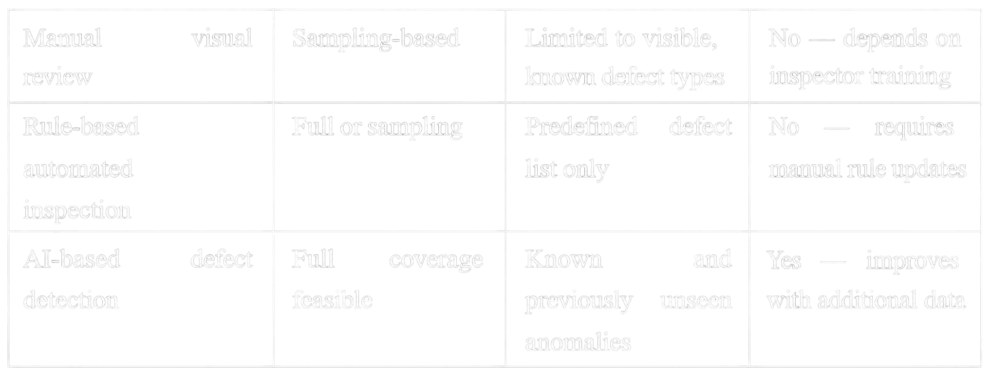
Manual and rule-based inspection methods are limited because the most critical defects are often novel and previously unobserved. Advancements such as new process nodes, materials, and packaging formats introduce defect types absent in earlier generations. Systems trained solely on a fixed catalog of known flaws will consistently overlook these emerging and frequently costly failure modes. AI-based semiconductor defect detection overcomes this limitation by learning the normal appearance of wafers or pattern layers directly from production data, enabling the identification of previously unseen anomalies without the need for pre-labeling every defect type.
Automated Semiconductor Quality Control in Production
Implementing automated semiconductor quality control in an operational fabrication facility requires integration of inspection decisions with the production line's control systems, rather than merely generating pass or fail image classifications. When an AI-based inspection model flags a wafer or die, the result must initiate a downstream action, such as rerouting the unit for engineering review, halting a process tool experiencing a defect spike, or logging the outcome for broader yield analysis.
This connects semiconductor inspection to a wider capability that xis.ai builds across its platform: centralized visibility across facilities. As covered in AI for Multi-Plant Quality Standardization, semiconductor manufacturing is one of the production environments where distributed facilities benefit from aggregated inspection data, since a defect pattern emerging at one fab can be identified and addressed at others before it repeats. The same underlying data acquisition principles that govern high-resolution defect imaging in other precision manufacturing contexts, discussed in Data Acquisition Techniques for AI-Based Inspection, apply directly to wafer-level imaging, where resolution, lighting, and capture consistency determine whether a model can reliably separate genuine defects from process noise.
Where AI-Based Inspection Fits Alongside Existing Systems
Semiconductor fabs rarely replace existing inspection infrastructure wholesale. AI-based defect detection is more commonly layered onto existing optical and SEM inspection tools, adding a trained classification and anomaly-detection step on top of image capture hardware that is already in place. This mirrors the broader distinction between machine vision and computer vision that shapes industrial inspection generally, explored in Machine Vision vs. Computer Vision: What's the Difference? , the imaging hardware defines what can be seen, while the AI model defines what can be understood from it.
As semiconductor manufacturing advances toward smaller process nodes, increased die density, and more complex packaging, critical defects increasingly fall outside the scope of fixed rule sets. Automated quality control systems based on AI models enable fabrication facilities to adapt to these changes without the need to re-engineer inspection lines for each new generation of defects.
Frequently Asked Questions
What is semiconductor defect detection?
Semiconductor defect detection is the process of identifying flaws on a wafer, die, or finished chip, such as particle contamination, pattern misalignment, or crystal-originated defects, at inspection checkpoints throughout fabrication and assembly.
How does AI improve semiconductor wafer inspection?
AI-based inspection learns the normal appearance of a wafer or pattern layer from production data, allowing it to flag previously unseen anomalies rather than relying only on a predefined list of known defect types.
What causes wafer surface defects?
Common causes include particle contamination during handling, photolithography pattern errors, crystal defects present in the substrate, mechanical damage from wafer handling, and non-uniform film deposition.
Can AI-based inspection replace existing fab inspection equipment?
Not typically. AI-based defect detection is usually layered onto existing optical and SEM inspection hardware, adding a trained classification step rather than replacing the imaging systems already in place.
Why does micro defect detection matter for yield?
Because a wafer carries a large volume of production value across many die, even small improvements in defect capture rate at the micron and sub-micron scale have an outsized effect on the proportion of die that pass final test.
Comment
0Comments
No comments yet.