AI-powered Precision Connector Quality Control

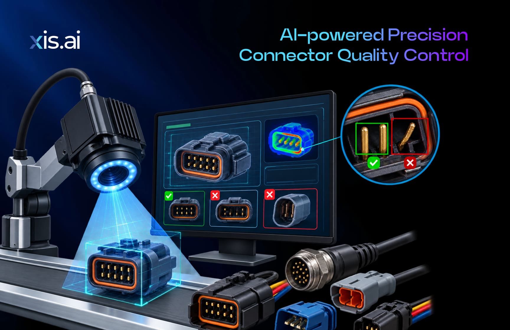
Electrical connectors look simple from the outside, but they concentrate a disproportionate share of assembly failures relative to their size. A connector's function depends on dozens of small mechanical tolerances holding at once: pin spacing, pin straightness, housing alignment, plating coverage, and seating depth all must fall within specification simultaneously for the connection to be reliable. A single bent pin or a fraction-of-a-millimeter misalignment will not always cause an immediate failure. It is just as likely to create an intermittent fault that surfaces after the product has shipped, which makes connector defects some of the costliest to catch late.
This is the core problem connector quality control has to solve: the defects that matter most are frequently the ones least visible to a human inspector working at normal assembly speed. Pin-level tolerances are difficult to judge by eye, connectors are often inspected from a single angle on the line, and high-volume production leaves little time for the kind of close visual review that would reliably catch a subtle bend or a partially seated terminal.
Solving for Pin Alignment Inspection
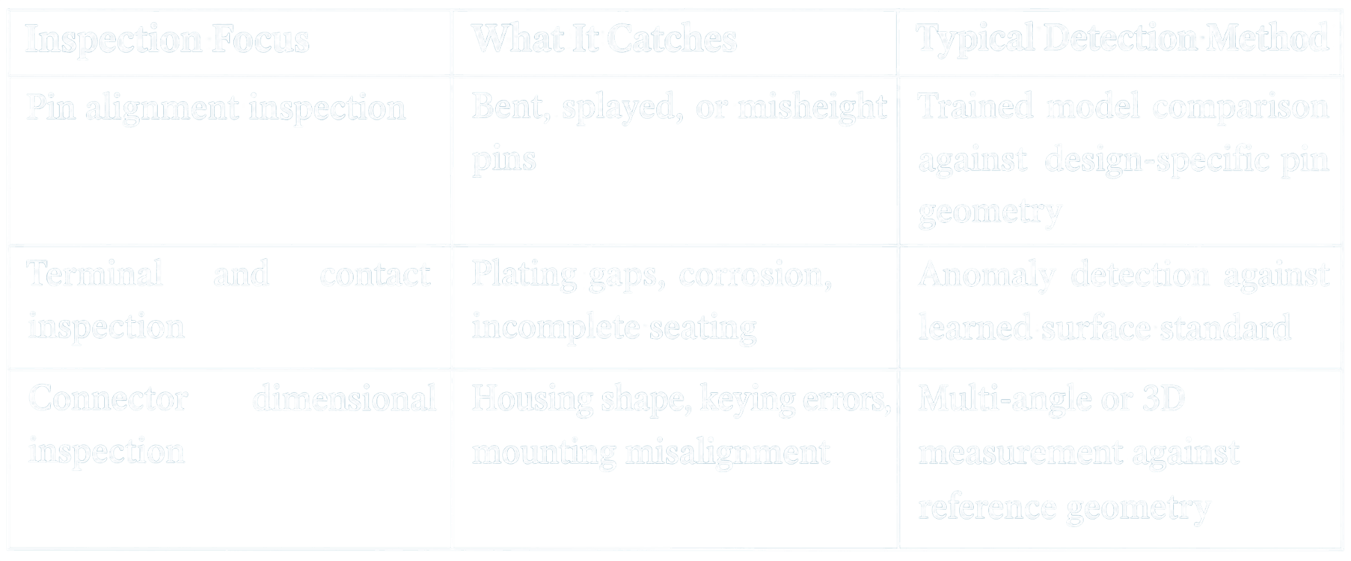
Pin alignment inspection is the first and most common failure point in connector quality control. Pins that are bent, splayed, or set at the wrong height relative to the housing will not mate correctly with a mating connector, and the resulting connection can range from immediately non-functional to intermittently unreliable depending on how far out of tolerance the pin sits.
AI-based connector pin inspection addresses this by training a model on the expected geometry of a specific connector design, then measuring every pin against that reference at production speed. Because the model is trained per connector design rather than working from a generic tolerance band, it accounts for the legitimate variation between different pin counts, pitches, and housing styles that a single fixed rule set would struggle to cover consistently. This same design-specific approach is what makes solder joint inspection effective at catching subtle placement issues, as covered in AI Solder Joint Inspection for Electronics Manufacturing — a trained model built around the specific characteristics of one component holds accuracy across the range of parts a manufacturer actually produces, rather than applying the same generic threshold to all of them.
Solving for Terminal and Contact Inspection
Terminal inspection covers a different set of failure modes than pin alignment: plating coverage, contact surface condition, and the physical seating of the terminal inside the housing. Insufficient plating on a contact surface increases resistance and accelerates corrosion at the connection point, while a terminal that has not fully seated can pass an initial visual check and still fail under vibration or thermal cycling once the product is in service.
Because these defects are often subtle changes in surface appearance rather than obvious geometric errors, terminal inspection benefits from the same anomaly-based detection method used elsewhere in electronics manufacturing: a model learns what a correctly plated, fully seated terminal looks like, then flags deviations from that learned standard automatically. This mirrors the approach detailed in AI SMT Inspection Systems: Why Electronics Manufacturers Are Rethinking Quality Control, where the same difficulty, catching defects that are small, subtle, and easy to miss under normal lighting and inspection speed, drives the case for AI-based detection over rule-based thresholds.
Solving for Connector Dimensional Inspection
Beyond individual pins and terminals, the connector housing itself carries dimensional requirements: overall shape, keying features that prevent incorrect mating, and mounting geometry that has to align with the board or cable assembly it connects to. Dimensional inspection at this level typically combines multiple imaging angles or 3D measurement to verify that the housing and its features fall within tolerance, since a single top-down image often cannot capture depth-related defects such as an under-seated connector body.
Why This Belongs on the Inspection Line, Not After It
The practical case for automated connector defect detection is timing. A connector defect caught during assembly, before the board or cable it belongs to advances further into production, is inexpensive to correct. The same defect caught during final product test, or worse, after a unit has shipped and failed in the field, carries the full cost of rework, warranty claims, and in some cases a broader recall investigation to determine how widespread the underlying issue is.
Full-coverage AI-based inspection changes the economics of when a connector defect gets caught. Rather than relying on periodic manual sampling, which by definition leaves most connectors on a production run unchecked, an AI-based system applies the same trained standard to every unit passing the inspection point. This full-coverage principle is the same one driving the broader shift away from manual sampling across electronics manufacturing generally, discussed in AI vs Manual Inspection: Accuracy, Speed, and ROI, where consistent full-line coverage, not just higher per-unit accuracy, is what most changes defect escape rates in practice.
Frequently Asked Questions
What causes most connector inspection failures?
Pin alignment errors, incomplete terminal seating, and plating defects are the most common causes, and most are difficult for a human inspector to catch reliably at normal assembly speed because the tolerances involved are small.
How does AI-based pin alignment inspection work?
A model is trained on the expected geometry of a specific connector design, then measures every pin on every unit against that reference at production speed, accounting for legitimate variation between connector styles rather than applying one fixed tolerance to all designs.
Why is terminal inspection difficult for rule-based systems?
Many terminal defects, such as incomplete seating or insufficient plating, are subtle changes in surface appearance rather than clear geometric errors, which makes them better suited to anomaly-based detection than fixed threshold rules.
Does connector inspection need more than one camera angle?
Often, yes. Depth-related defects such as an under-seated connector body or misaligned housing feature are not reliably visible from a single top-down image, so multi-angle or 3D measurement is used for dimensional inspection.
Why does catching connector defects early matter so much?
A connector defect corrected during assembly is inexpensive. The same defect caught after final test or after a product ships carries the added cost of rework, warranty claims, and potential field failure investigation.
Comment
0Comments
No comments yet.